About American Precision Dicing
Established in 1999, American Precision Dicing, Inc. (APD) is a semiconductor services company located in San Jose, California, in the heart of Silicon Valley. APD operates from 642 Giguere Court and supports customers who require precise, responsive, and reliable wafer processing for research, prototyping, and production applications.
Our team works with a wide range of customers, including universities, hardware startups, private and federal research laboratories, defense contractors, and major semiconductor corporations.
Precision Wafer Processing in Silicon Valley
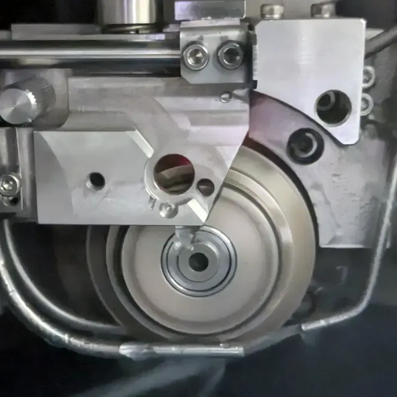
APD uses precision mechanical dicing saws equipped with diamond blades to process a wide range of hard and brittle materials. Our process knowledge allows us to support standard and specialized requirements, including small research lots, prototype development, and low to medium volume production.
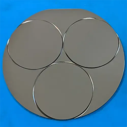
We routinely process semiconductor, optical, ceramic, and composite substrates such as:
- Silicon
- Gallium arsenide
- Glass
- Quartz
- Ceramics
- Alumina
- Sapphire
- Silicon carbide
- FR4 and printed circuit board (PCB) materials
- Other hard and brittle substrates
Related Wafer Processing and Post-Dicing Support
While wafer dicing is our core competency, APD also provides related singulation and post-dicing support. Our capabilities include
wafer dicing,
wafer coring, and
PCB depanelization.
We also offer specialized processing and die handling services, including die sort, pick and place, and labeling, photoresist application and removal, wafer backgrinding and laser marking.
Quality, Security, and Certifications
Because APD serves semiconductor, aerospace, defense, research, and advanced technology customers, we maintain quality and compliance practices designed to support sensitive wafer processing projects.

APD maintains an ISO 9001:2015 certified Quality Management System. Our processes are documented, repeatable, and traceable to support consistent customer requirements.
APD is registered under the International Traffic in Arms Regulations (ITAR). ITAR registration documentation and compliance details are available to verified customers upon request.
What We Do
APD provides a diverse range of services, expertly developed in-house or managed in collaboration with our trusted long-term partners.
Wafer Dicing Service
Precision dicing of wafers is our core expertise, driven by decades of experience and technological innovation.
Wafer Coring
Expert resizing of wafers to meet specific diameter requirements, ensuring optimal performance.
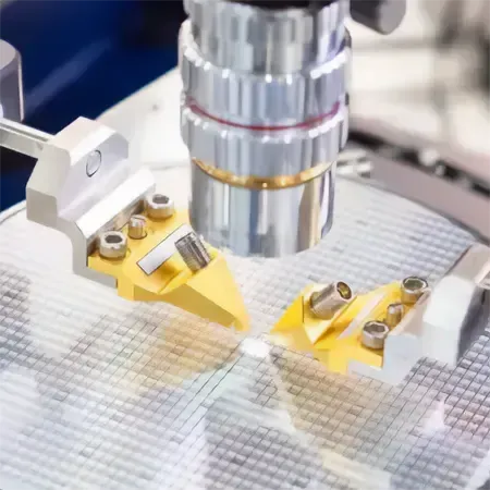
Die Sort, Pick & Place
Optimizing wafer processing with meticulous sorting, pick & place, and labeling.
Laser Marking
Utilizing advanced laser technology for precise and permanent serial number etching on wafers.
Photoresist
Safeguarding wafers with a photoresist layer during subsequent manufacturing steps.
Wafer Dicing Service
Precision dicing of wafers is our core expertise, driven by decades of experience and technological innovation.
Wafer Coring
Expert resizing of wafers to meet specific diameter requirements, ensuring optimal performance.
Our Service Principles
At APD, we prioritize speed, value, and flexibility. These principles guide our commitment to delivering exceptional wafer dicing services, ensuring efficient, cost-effective, and customized solutions for our clients.

Speed
For urgent wafer dicing, we provide same-day service and assure next-day shipping with overnight delivery. Our skilled team, coupled with advanced cutting machines, ensures maximum efficiency.

Value
When dicing wafers, speed and experience are essential factors in maximizing efficiency and accuracy with a high cutting speed to reduce costs.

Flexibility
Our company promises to offer customized solutions for each customer that fits their needs. We offer tailored solutions to meet the needs of our customers.
Our Valued Customers
Our valued customers include leading companies, research labs, and universities who trust us for their wafer dicing and processing needs.